Professor Yongtaek Hong’s Research Team at Seoul National University Develops ‘Selective Metal Films Deposition Technique’ Enabling Fabrication of Soft Electronics with Various Form Factors
- Increases applicability of highly conductive evaporated metal thin films in soft electronics including curvilinear OLEDs and stretchable LED arrays
- Published in the world-renowned scientific journal Nature Communications

(From left) Dr. Sujin Jeong, Dr. Hyungsoo Yoon, Prof. Yongtaek Hong from the Department of Electrical and Computer Engineering at Seoul National University, and Prof. Byeongmoon Lee from the Department of Electrical Engineering and Computer Science at DGIST.
Seoul National University’s College of Engineering announced that a research team led by Prof. Yongtaek Hong from the Department of Electrical and Computer Engineering, in collaboration with Prof. Byeongmoon Lee from the Department of Electrical Engineering and Computer Science at the Daegu Gyeongbuk Institute of Science and Technology (DGIST), has developed a ‘printing-based selective metal film deposition technique’ that enables the facile and fast fabrication of high-performance soft electronic devices and circuits in various forms.
The results of this research were published on the 22nd of August in Nature Communications, a prestigious international scientific journal.
Metal thin films formed using vapor deposition have excellent electrical conductivity and surface quality, making them key components of electronic devices and circuits. However, patterning these metal thin films into desired shapes typically requires the use of rigid masks such as shadow masks or photomasks, which makes it difficult to modify patterns and limits the ability to carry out processes on surfaces of various forms.
To address this issue, the research team developed a 'printing-based selective metal thin film deposition technique.' This method utilizes polymer patterns to block the condensation of metal vapor, allowing the vapor deposition and patterning processes to be performed at the same time without the need for a separate mask. This approach enables the production of patterns with line widths ranging from micrometers (μm) to millimeters (mm) on a large scale.
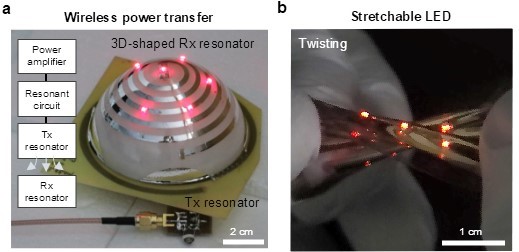
According to the research team, the polymer pattern’s excellent stretchability and mechanical durability allow metal thin film patterns to be easily formed on multi-curvature or elastic substrates, which were previously impossible with conventional methods. During the research, they demonstrated next-generation free-form electronic devices and circuits, including wireless power transmission, curvilinear OLEDs (Organic Light Emitting Diodes), and stretchable LED arrays, by using metal thin films in various shapes.
Prof. Yongtaek Hong highlighted the significance of the research, stating, “This study not only developed a technology for easily custom-fabricating high-performance metal thin film patterns based on vapor deposition, but also set the stage for maximizing the utility of metal thin films in the field of soft electronics by applying this technology to curved and stretchable systems.” He added, “In the future, this selective metal thin film deposition technology is expected to be directly applied to forming porous transparent structures in the top common electrode of OLED panels, a key element for under-display camera and under-display face recognition sensor technologies that require various form factors.”
Meanwhile, Dr. Sujin Jeong and Dr. Hyungsoo Yoon, co-first authors of the paper, are currently working at Samsung Display Research Center, focusing on the development of next-generation future displays, including stretchable displays. The research was supported by the Ministry of Science and ICT.

Figure 1: Metal thin film patterns on (left to right) 2D planar, 3D curvilinear, and stretchable substrates

Figure 2: (a) Demonstration of wireless power transfer (b) Demonstration of stretchable light-emitting diode
[Reference materials]
https://www.nature.com/articles/s41467-024-51585-2
[Contact Information]
Prof. Yongtaek Hong, Department of Electrical and Computer Engineering, Seoul National University
Email: yongtaek@snu.ac.kr
Phone: +82-2-880-9567


